Why I am not an experimentalist; or, making faces with photolithography
In 2019, I spent six months in Gothenburg, Sweden at the Chalmers Institute of Technology. I was working in the lab of Per Delsing doing nanofabrication in my gap year before grad school, and it was not going well.
Have you ever wondered how computer chips are made? A chip is basically a block of silicon covered in an immense tangle of thin wires and pieces of doped silicon. These wires are absolutely tiny, just nanometers wide, which is way smaller than the spatial resolution of any machine we could use to mechanically lay down the wires.
To get around that and get all those wires down, you use a bewildering combination of chemistry and particle physics. First you cover the slab of silicon with a thin layer of a substance called “resist.” The resist is sensitive to either photons or electrons, so you shine either a laser or an electron beam over the slab where you want wires to go. You can then wash away the irradiated resist, exposing the bare silicon underneath, and just cover the whole thing with a thin layer of metal shot in from above. The resist blocks the metal everywhere but in the wire tracks, so when you wash away the rest of the resist, you’re left with nice, beautiful wires. Here’s a cartoon I drew:
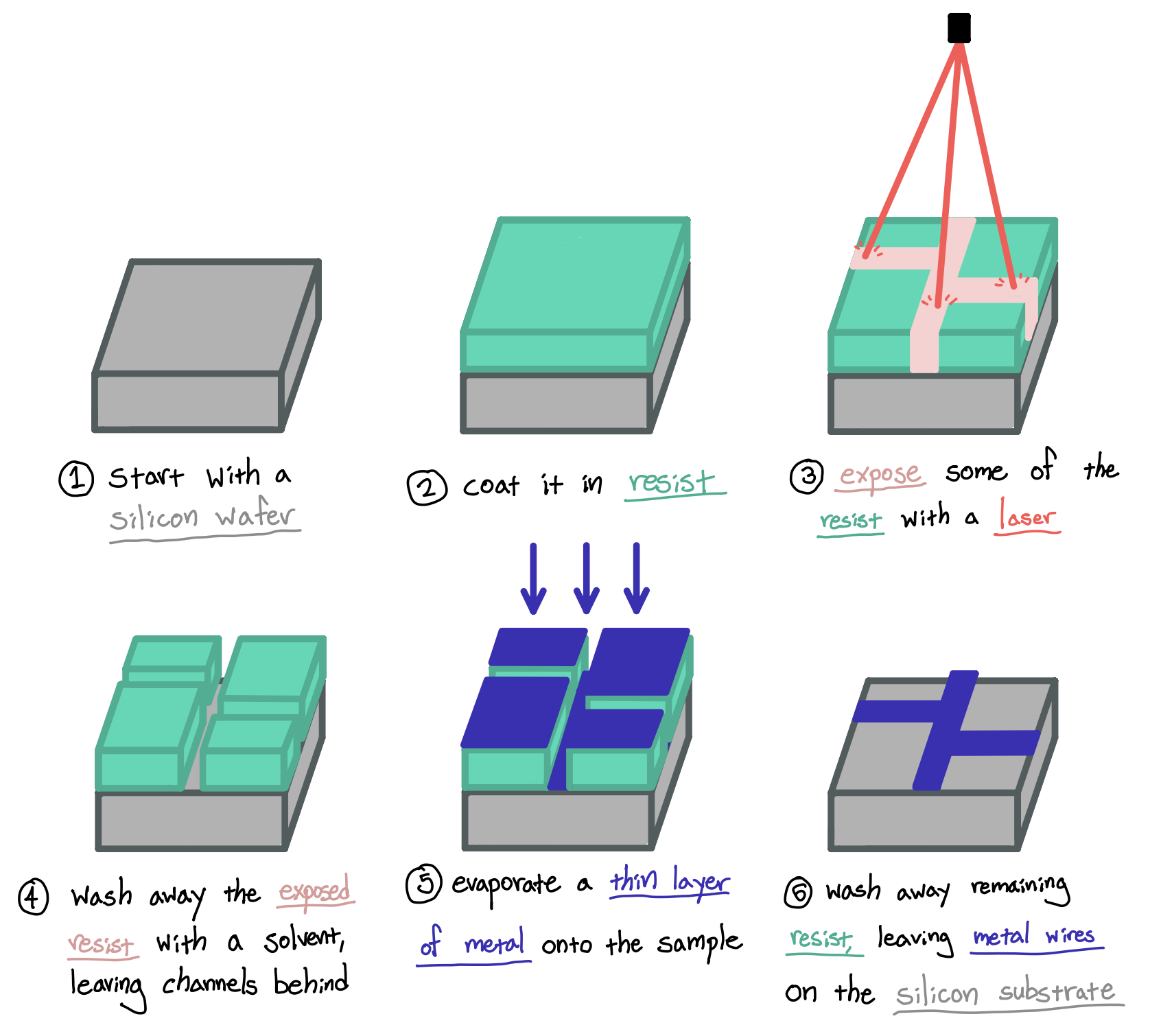
With this technique and variations on it, all modern computer chips are manufactured. My job that fateful summer was to use this technique to design quantum inductors, and I was rapidly learning that I was not cut out for labwork. Every step in the cartoon above is actually ten different steps involving mixing toxic chemicals, heating things, putting things into big scary machines, and using inscrutable computer interfaces with a hundred settings. Oh, and to make matters worse, you have to do all this while sweating inside a head-to-toe cleanroom lab suit. My mentor, Anita, would demonstrate something with practiced care and deliberation, she’d walk away, and I would promptly forget everything except maybe what colors were supposed to be created. I cannot overstate the extent of my incompetence: on several occasions, I left a piece of support plastic called a “spider” on a hot plate and literally melted it to the piece of silicon I was working with. This continued until Anita told me to stop using spiders.
Even though I was close to useless in the lab, it turned out I was pretty good at coming up with things for other people to try. At the start of my time there, I learned that quantum inductors are usually made with three shoot-down-a-layer-of-metal steps to make three different parts of the circuit. You can do the first two in one machine cycle, but for annoying geometric reasons, everyone did the third step in its own cycle, which could take an extra day or two. I found a way to do them all in one machine cycle by shooting the metal down from three different angles. Thanks to the hard work of my collaborators to show this idea actually worked — figuring out how to fabricate the design, characterize it, and test it in quantum circuits — this is now among my most-cited publications. The finished quantum inductors looked like this:
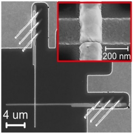
A Josephson junction made with our speedy fab process.
And now we get to my favorite part of this story. Our silicon wafers were about two inches wide. They’re pretty expensive, so you don’t want to waste them, but you only ever end up using about two thirds of the surface area since you want to leave the borders clear so you can grab the thing with tweezers. This leaves a lot of room for you to print tests or calibration marks, and this fact was not lost on me. Do you see where I’m going with this?
It was not too long until I realized that the time it took to pattern something onto the silicon was proportional to its size, not its complexity, so I could print really complicated stuff, and whatever I wanted, onto the edges of these wafers, so long as it was small. So I figured out how scripting worked in the design software, and I wrote some Python to break images down into a format suitable for this software, and then I could print whatever I wanted in a nanometers-thick layer of aluminum. Naturally, the first thing I printed was my professor’s head:
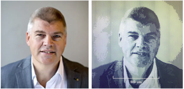
Left: Professor Per Delsing. Right: Professor Per Delsing on silico.
I left this image up on his door. I’m pretty sure he knew it was me, but we never talked about it. I also printed my own head and a picture with some of my friends:
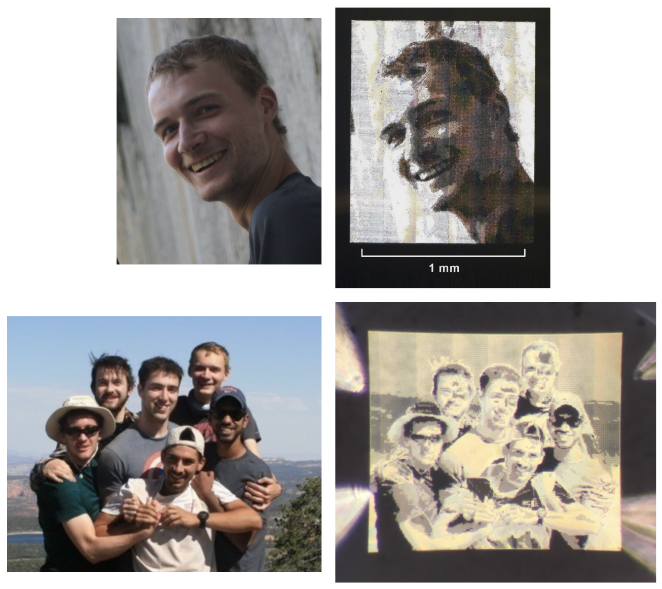
Top: me. Bottom: me and friends.
It’s pretty fun to be able to fabricate things at such a small scale. Each of these images has a total size of about 1mm. I still have the picture of myself, and I own a little microscope I can use to look at it. I used it on my dating profile for a while until I conceded nobody knew what the hell they were looking at and gave up.
In August 2019, I left Sweden and started my PhD at Berkeley. I switched gears away from experiment, and then away from quantum physics altogether, and joined a lab studying, among other things, the fundamental theory of deep learning, and that got me to where I am today. But now, as I use a computer, and run things with GPUs, and stand by as tech giants fill warehouses with upwards of millions of GPUs and $10^{17}$ transistors total, it’s illuminating and remarkable and a deeply privileged feeling to have gotten to see how computer chips are made.